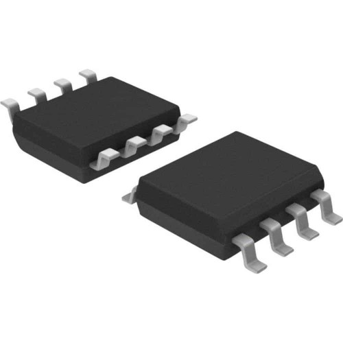
ACS712 20 Ampere IC
-
Rs.
199.42 (inc GST)
Rs.169.00 + GSTQty :
GST Invoice on all Purchase. So you will be eligible to take input tax credit. |
IF component not in Stock or require more quantity or want to buy in bulk e-mail us your requirements on: dnatechindia "at" gmail.com. |
| Shipping : Due to Covid-19 situation delivery will be affected. Delivery period due to covid-19 issue will be from 4 - 12 days depending upon your location. |
ACS712 20 Ampere Current Sensor IC
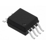
ACS712ELCTR-20A-T - ACS712 20 Ampere Hall Effect Based Linear Current Sensor IC
The Allegro ACS712 provides economical and precise solutions for AC or DC current sensing in industrial, commercial, and communications systems. The device package allows for easy implementation by the customer. Typical applications include motor control, load detection and management, switched-mode power supplies, and over current fault protection.
The ACS712ELCTR-20A-T provides current measurement upto 20 Ampere for both AC as well as DC current.
ACS712 current sensor IC consists of a precise, low-offset, linear Hall sensor circuit with a copper conduction path located near the surface of the die. Applied current flowing through this copper conduction path generates a magnetic field which is sensed by the integrated Hall IC and converted into a proportional voltage. Device accuracy is optimized through the close proximity of the magnetic signal to the Hall transducer. A precise, proportional voltage is provided by the low-offset, chopper-stabilized BiCMOS Hall IC, which is programmed for accuracy after packaging.
The output of the device has a positive slope (>VIOUT(Q)) when an increasing current flows through the primary copper conduction path (from pins 1 and 2, to pins 3 and 4), which is the path used for current sensing. The internal resistance of this conductive path is 1.2 mΩ typical, providing low power loss. The thickness of the copper conductor allows survival of the device at up to 5× overcurrent conditions. The terminals of the conductive path are electrically isolated from the sensor IC leads (pins 5 through 8). This allows the ACS712 current sensor IC to be used in applications requiring electrical isolation without the use of optoisolators or other costly isolation techniques.
The ACS712 is provided in a small, surface mount SOIC8 package. The lead frame is plated with 100% matte tin, which is compatible with standard lead (Pb) free printed circuit board assembly processes. Internally, the device is Pb-free, except for flip-chip high-temperature Pb-based solder balls, currently exempt from RoHS. The device is fully calibrated prior to shipment from the factory.
Features of ACS712 SMD Current Sensor IC
- Low-noise analog signal path
- Device bandwidth is set via the new FILTER pin
- 5 µs output rise time in response to step input current
- 80 kHz bandwidth
- Total output error 1.5% at TA= 25°C
- Small footprint, low-profile SOIC8 package
- 1.2 mΩ internal conductor resistance
- 2.1 kVRMS minimum isolation voltage from pins 1-4 to pins 5-8
- 5.0 Volt , single supply operation
- 66 to 185 mV/A output sensitivity
- Output voltage proportional to AC or DC currents
- Factory-trimmed for accuracy
- Extremely stable output offset voltage
- Nearly zero magnetic hysteresis
- Ratiometric output from supply voltage
Additional Information for ACS712 IC
- Supply Voltage : 5.0 Volts
- Supply Current : 10 mA
- Primary Conductor Resistance : 1.2 mOhm
- Frequency Bandwidth : 80kHz
- Rise Time : 5us
- Output Capacitance Load : 10nF
- Power-On Time : 35us
- Optimized Accuracy Range : -20~20A
- Sensitivity : 100 mV/A
Related links
Package Includes
- 1 x ACS712 20 Ampere IC
NEW Products
Product Page : New Products
Winsen ZE03-SO2 GAS Sensor Module
Winsen ZE03-SO2 GAS Sensor ModuleElectrochemical Detection Module ZE03-SO2ZE03-SO2 Gas sensor can be..
Rs.13,216.00 (inc GST)
Rs.11,200.00 + GST
SKU: 1764 | DAB100
Stock: 2
H9700 2 channel Digital Output Small Optical Encoder Module
H9700 2 channel Digital Output Small Optical Encoder ModuleH9700 Unipolar Hall-Effect Sensor ICThe H..
Rs.1,652.00 (inc GST)
Rs.1,400.00 + GST
SKU: 7439 | DAF661
Stock: 3
DTECH IOT5064A RS485 Serial to Ethernet Converter Bluetooth adapter
DTECH IOT5064A RS485 Serial to Ethernet Converter Bluetooth adapterDTECH IOT5064A RS485 Serial to Et..
Rs.6,486.76 (inc GST)
Rs.5,497.25 + GST
SKU: 7466 | DAG852
Stock: 1
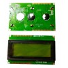
JHD 204 20X4 GREEN LCD DISPLAY CHINESSE
JHD 204 20X4 GREEN LCD DISPLAY CHINESSEJHD 204 20X4 GREEN LCD DISPLAY CHINESSEThis is a 20x4 LCD dis..
Rs.402.09 (inc GST)
Rs.340.75 + GST
SKU: 7663 | DAF077
Stock: 5
Have You Seen
Product Page : Have You Seen
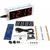
4 Digit DIY Electronic Clock kit Multicolor LED time Week Temperature Date Display with Clear case Cover (blue)
4 Digit DIY Electronic Clock kit Multicolor LED time Week Temperature Date Display with Clear case C..
Rs.796.50 (inc GST)
Rs.675.00 + GST
SKU: 7443 | DAF836
Stock: 5
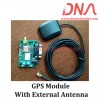
GPS Module With External Antenna
GPS Module With External AntennaThis is a GPS Module with External Antenna. It is based on Skytra S1..
Rs.1,180.00 (inc GST)
Rs.1,000.00 + GST
SKU: 0397 | DAE263
Stock: 0
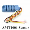
AMT1001 Resistive Temperature And Humidity Sensor
AMT1001 Resistive Temperature And Humidity SensorAMT1001 Resistive Humidity and Temperature Sensor M..
Rs.335.12 (inc GST)
Rs.284.00 + GST
SKU: 3291 | DAD402
Stock: 9
ADS1256 24bit High Precision ADC STM32F103C8T6 Module
ADS1256 24bit High Precision ADC STM32F103C8T6 ModuleADS1256 24bit High Precision ADC STM32F103C8T6 ..
Rs.5,198.70 (inc GST)
Rs.4,405.67 + GST
SKU: 7630 | DAF121
Stock: 0
Related Products
ACS712 20 Amp Current Sensor Module
ACS712 20 Amp Current Sensor ModuleACS712 20 Ampere Hall effect current Sensor Module This is a..
Rs.97.94 (inc GST)
Rs.83.00 + GST
SKU: 0264 | DAA680
Stock: 3
ACS712 5 Ampere IC
ACS712 5 Ampere Current Sensor IC ACS712ELCTR-05B-T - ACS712 5 Ampere Hall Effect Based Linear Curr..
Rs.199.42 (inc GST)
Rs.169.00 + GST
SKU: 2316 | DAB899
Stock: 0
ACS712 30 Ampere IC
ACS712 30 Ampere SMD Current Sensor IC ACS712ELCTR-30A-T - ACS712 30 Ampere Hall Effect Based Linea..
Rs.199.42 (inc GST)
Rs.169.00 + GST
SKU: 2326 | DAB901
Stock: 20
ACPLC790 500E Precision Miniature Isolation Amplifier IC
ACPLC790 500E Precision Miniature Isolation Amplifier ICACPLC790 500E SMD ICThe ACPLC790 500E is a h..
Rs.789.31 (inc GST)
Rs.668.91 + GST

