AD711 BiFET Opamp
- Stock: 5 InStock
- SKU: 0456 | DAA013
-
Rs.
365.80 (inc GST)
Rs.310.00 + GSTQty :
GST Invoice on all Purchase. So you will be eligible to take input tax credit. |
IF component not in Stock or require more quantity or want to buy in bulk e-mail us your requirements on: dnatechindia "at" gmail.com. |
| Shipping : Due to Covid-19 situation delivery will be affected. Delivery period due to covid-19 issue will be from 4 - 12 days depending upon your location. |
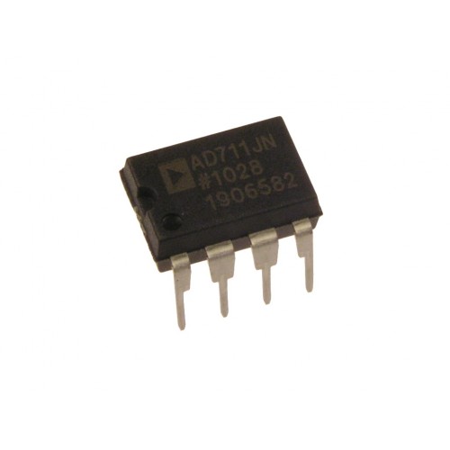
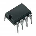
AD711 BiFET Opamp
AD711 Low Cost BiFET OPAMP
The AD711 is a high speed, precision monolithic operational amplifier offering high performance at very modest prices. Its very low offset voltage and offset voltage drift are the results of advanced laser wafer trimming technology. These performance benefits allow the user to easily upgrade existing designs that use older precision BiFETs and, in many cases, bipolar op amps.The superior ac and dc performance of this op amp makes it suitable for active filter applications. With a slew rate of 16 V/µs and a settling time of 1 µs to ±0.01%, the AD711 is ideal as a buffer for 12-bit D/A and A/D Converters and as a high-speed integrator. The settling time is unmatched by any similar IC amplifier.
The combination of excellent noise performance and low input current also make the AD711 useful for photo diode preamps. Common-mode rejection of 88 dB and open loop gain of 400 V/mV ensure 12-bit performance even in high-speed unity gain buffer circuits.
HIGHLIGHTS of AD711
- The AD711 offers excellent overall performance at very competitive prices.
- Analog Devices’ advanced processing technology and 100% testing guarantee a low input offset voltage (0.25 mV max, C grade, 2 mV max, J grade). Input offset voltage is specified in the warmed-up condition. Analog Devices’ laser wafer drift trimming process reduces input offset voltage drifts to 3 mV/∞C max on the AD711C.
- Along with precision dc performance, the AD711 offers excellent dynamic response. It settles to ±0.01% in 1 ms and has a 100% tested minimum slew rate of 16 V/ms. Thus this device is ideal for applications such as DAC and ADC buffers which require a combination of superior ac and dc performance.
- The AD711 has a guaranteed and tested maximum voltage noise of 4 mV p-p, 0.1 to 10 Hz (AD711C).
- Analog Devices’ well-matched, ion-implanted JFETs ensure a guaranteed input bias current (at either input) of 25 pA max (AD711C) and an input offset current of 10 pA max (AD711C). Both input bias current and input offset current are guaranteed in the warmed-up condition.
Features of AD711 BiFET OPAMP
- Enhanced Replacement for LF411 and TL081
- AC PERFORMANCE
- Settles to 0.01% in 1.0 s
- 16 V/s min Slew Rate (AD711J)
- 3 MHz min Unity Gain Bandwidth (AD711J)
- DC PERFORMANCE
- 0.25 mV max Offset Voltage: (AD711C)
- 3 V/C max Drift: (AD711C)
- 200 V/mV min Open-Loop Gain (AD711K)
- 4 V p-p max Noise, 0.1 Hz to 10 Hz (AD711C)
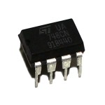
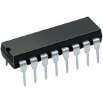
- Available in Plastic Mini-DIP, Plastic SOIC, HermeticCerdip, and Hermetic Metal Can Packages
Related Link
NEW Products
Product Page : New Products
Winsen ZE03-SO2 GAS Sensor Module
Winsen ZE03-SO2 GAS Sensor ModuleElectrochemical Detection Module ZE03-SO2ZE03-SO2 Gas sensor can be..
Rs.13,216.00 (inc GST)
Rs.11,200.00 + GST
SKU: 1764 | DAB100
Stock: 2
H9700 2 channel Digital Output Small Optical Encoder Module
H9700 2 channel Digital Output Small Optical Encoder ModuleH9700 Unipolar Hall-Effect Sensor ICThe H..
Rs.1,652.00 (inc GST)
Rs.1,400.00 + GST
SKU: 7439 | DAF661
Stock: 3
DTECH IOT5064A RS485 Serial to Ethernet Converter Bluetooth adapter
DTECH IOT5064A RS485 Serial to Ethernet Converter Bluetooth adapterDTECH IOT5064A RS485 Serial to Et..
Rs.6,486.76 (inc GST)
Rs.5,497.25 + GST
SKU: 7466 | DAG852
Stock: 1
JHD 204 20X4 GREEN LCD DISPLAY CHINESSE
JHD 204 20X4 GREEN LCD DISPLAY CHINESSEJHD 204 20X4 GREEN LCD DISPLAY CHINESSEThis is a 20x4 LCD dis..
Rs.402.09 (inc GST)
Rs.340.75 + GST
SKU: 7663 | DAF077
Stock: 5
Have You Seen
Product Page : Have You Seen
4 Digit DIY Electronic Clock kit Multicolor LED time Week Temperature Date Display with Clear case Cover (blue)
4 Digit DIY Electronic Clock kit Multicolor LED time Week Temperature Date Display with Clear case C..
Rs.796.50 (inc GST)
Rs.675.00 + GST
SKU: 7443 | DAF836
Stock: 5
GPS Module With External Antenna
GPS Module With External AntennaThis is a GPS Module with External Antenna. It is based on Skytra S1..
Rs.1,180.00 (inc GST)
Rs.1,000.00 + GST
SKU: 0397 | DAE263
Stock: 0
AMT1001 Resistive Temperature And Humidity Sensor
AMT1001 Resistive Temperature And Humidity SensorAMT1001 Resistive Humidity and Temperature Sensor M..
Rs.335.12 (inc GST)
Rs.284.00 + GST
SKU: 3291 | DAD402
Stock: 9
ADS1256 24bit High Precision ADC STM32F103C8T6 Module
ADS1256 24bit High Precision ADC STM32F103C8T6 ModuleADS1256 24bit High Precision ADC STM32F103C8T6 ..
Rs.5,198.70 (inc GST)
Rs.4,405.67 + GST
SKU: 7630 | DAF121
Stock: 0
Related Products
LM311 Comparator
LM311 ComparatorThe LM311 is single high-speed voltage comparators. These devices are designed to op..
Rs.20.06 (inc GST)
Rs.17.00 + GST
SKU: 0558 | DAA079
Stock: 21
OP37G High Speed Op-Amp
OP37G High Speed Op-AmpThe OP37 op-amp provides the low offset and drift of the OP07 ..
Rs.153.40 (inc GST)
Rs.130.00 + GST
SKU: 0808 | DAB577
Stock: 0
LM748 Op-Amp
LM748 Op-AmpThe LM748 is a general purpose operational amplifier with external frequency compensatio..
Rs.22.42 (inc GST)
Rs.19.00 + GST
SKU: 0809 | DAA073
Stock: 5
AD526 Digitally Programmable Gain Amplifier
AD526 Gain AmplifierAD526 Digitally Programmable Gain AmplifierThe AD526 is a single-ended, monolith..
Rs.706.82 (inc GST)
Rs.599.00 + GST
SKU: 0968 | DAA002
Stock: 1
OP07 Precision SMD OPAMP
OP07 Precision OPAMPOP07 Precision OPAMP SMD ICThe OP07 (Operational Amplifier) has very low in..
Rs.16.52 (inc GST)
Rs.14.00 + GST
SKU: 7234 | DAD542
Stock: 1000
TS9222IYDT IC OPAMP GP 2 CIRCUIT 8SOIC
TS9222IYDT IC OPAMP GP 2 CIRCUIT 8SOICTS9222IYDT IC OPAMP GP 2 CIRCUIT 8SOICThe TS9222IYDT IC O..
Rs.233.88 (inc GST)
Rs.198.20 + GST
SKU: 7331 | DAG324
Stock: 0
FD2103S SMD GATE DRIVER IC
FD2103S SMD GATE DRIVER ICFD2103S SMD GATE DRIVER ICThe FD2103S is a half-bridge gate driver IC deve..
Rs.36.34 (inc GST)
Rs.30.80 + GST
SKU: 8130 | DAH635
Stock: 48
Tags: Op-Amp

