Different Types of Printed Circuit board Explained
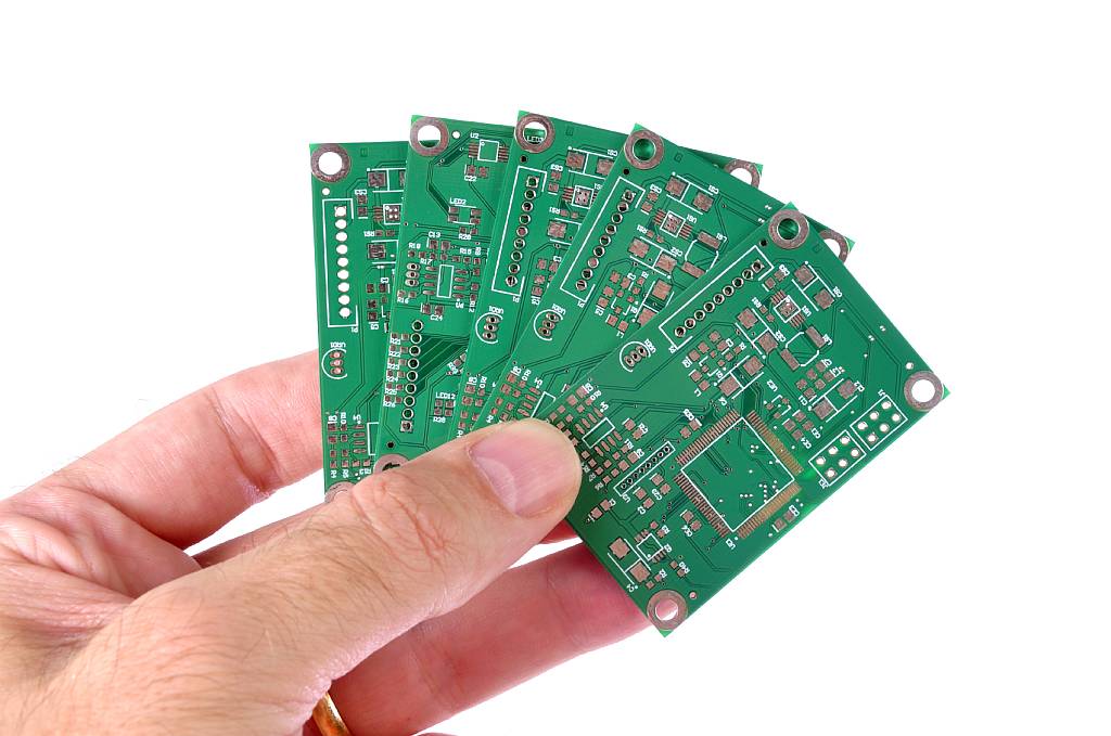
An electronic circuit consists of various active and passive components like resistors, inductor's, led’s, transistors, MOSFETS and IC’s. For running a circuit all components can be mounted on a breadboard or Zero/Dotted or General PurposePCB’s where they are electrically connected together by wires. The components can also be mounted on a customised Printed circuit Board in which specially designed copper tracks have been provided for electrically connecting different components.

What is PCB?
PCB is an acronym for Printed Circuit Board it is a board that connects various points of the circuit together and allows signals and power to be routed between different components. A bare PCB is also called as
copper clad. Earlier circuits were made using point to point wiring which made them time consuming to manufacture, very difficult to debug and prone to failures.
As technology improved components became smaller also there was need for large scale production as well as cost reduction all these were major factors that lead to the concept of PCB being born. If you are interested in knowing the History of PCB do check out this
link.
PCB Board is one of the most basic part of any electronic circuit. Just remember that any electronic device/product/part in a product is always mounted on a PCB.
A PCB board is etched from bare PCB also called as Copper clad which are basically copper sheets laminated onto a non-conductive substrate. A bare Copper clad consists of two parts

The base material also called Substrate or laminate is a non-conductive layer provides strength & flexibility to the PCB. Various materials are used as substrate later in this article we will discuss the material used for substrate. This base material can be flexible as well.
The copper sheet or copper foil is the conductive part of the PCB and it is this part that allows current to flow through the circuit. Other Conductive material like stainless steel,beryllium copper or nickel can also be used but copper is used extensively because it is easily available and comparatively is low costing.
A copper clad can be classified based upon various parameters/factors
- Base Material Used
- Thickness of Copper foil
- Number of Layers
Base Material Used
The base material provides insulation, mechanical strength, stability and rigidity to the copper clad. Two of the most common type of base material used are:
These PCB material are known as FR1 & FR2 PCB. In this type of PCB Paper (mixture of wood fiber and phenolic polymers) is used as a reinforcement. Paper Phenolic PCB is mostly brown in colour. They are low cost but have tendency to absorb moisture and they crack/shears easily. They are used mostly by students, hobbyist and in products where cost is a big factor. These PCB material are known as FR4 PCB in these type of PCB fiber glass is used as base material. Glass Epoxy PCB's are generally greenish in colour. Glass epoxy PCB have near zero water absorption, chemical resistant, flame resistant and have higher electrical insulating qualities. They are costlier than paper phenolic PCB.
Copper foil Thickness
The conductive layer of a PCB is made of copper. The thickness of the copper is usually expressed in ounces per square foot. Well it is odd isn't it? Copper thickness is being measured in ounce. In PCB terminology 1 ounce/square ft is equivalent to 35 microns (1 micron is one millionth of a meter) similarly 2 ounce/square ft is equivalent to 70 microns.
As the thickness of the copper foil increases its resistivity decreases meaning lesser loss and lesser heating of tracks. But the price of the copper clad increases as the thickness increases. So according to your application you decide the copper foil thickness.
Most of the commonly used PCB's have copper thickness of 18 micron. And if you want to reduce cost further you can get PCB's up-to 12 micron thickness. So depending on your application you can select the foil thickness of your copper clad.
Number of Layers
PCB's can also be classified based on the number of copper layers on one PCB.
In single sided PCB there is only one layer of copper foil and one layer of substrate. Normally in a single sided PCB there is top side and bottom side. Top side is where through hole components are mounted and the bottom side is where soldering of components leads are done. SMD components are also soldered on bottom side.

Single sided PCB's are low cost and very easy to manufacture, test and debug. These are so easy to manufacture that you can manufacture them at your home with some basic raw material.

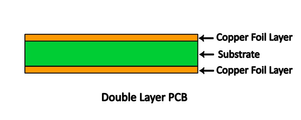
Double sided PCB's are a bit difficult to manufacture. In this type there is only one base material but there are two copper layers one on both sides of the base material. So basically both sides of Double sided PCB's are conductive and electronic components can be placed as well as soldered on both sides of the PCB. There are tracks on both sides of the PCB and are connected together using PTH technology.
What exactly is PTH PCB?
PTH is an abbreviation for "Plated through Holes". In double/multi layer PCB's for connecting tracks electrically on different layers of the board drill holes with conductive material are made. These conductive holes are also called as Vias. These PTH Connections either form simple electrical connection between both sides of the PCB (Via Holes), or electrical connectivity and also provide good mechanical support for leaded components. This makes the double sided PTH PCB a much more physically robust item.
Though you can make a double sided PCB without PTH as well. These type of PCB is called as Double sided non-PTH PCB. These types of PCB's are rarely used. In this case the electrical connection between the two layers is done by manually i.e. placing a link (normally a resistor leg is used) in a drill hole and then soldering on both sides of the board.
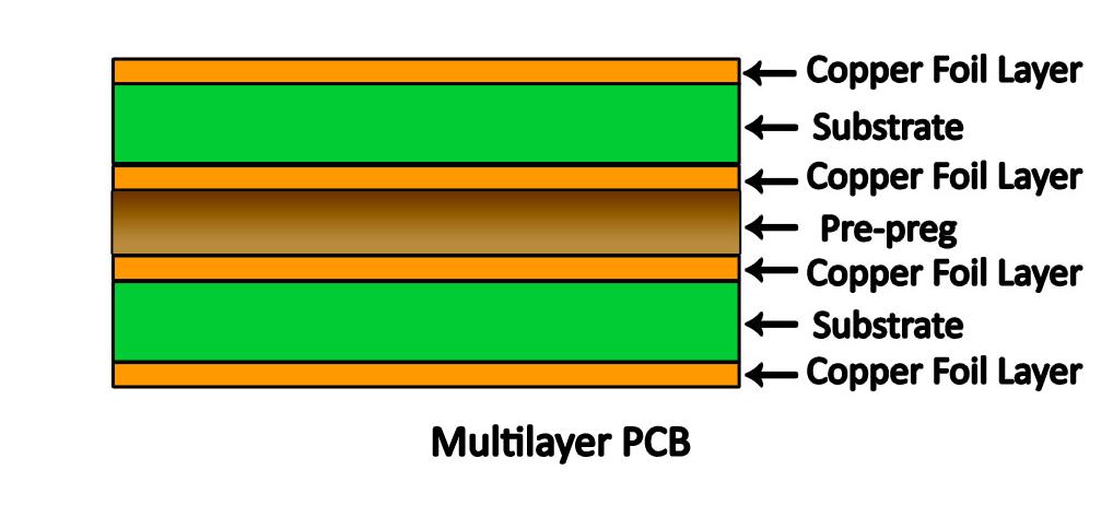
Multi lever PCB's are the upper version of double sided PCB. In this type more than two copper layers are there on a single PCB. Multi-layer PCB provides designers to manufacture very complex and compact circuits having high component density.

A multi layer PCB is basically multiple double sided PCB which are bonded together with a special glue called as pre-leg. In multi layer PCB's separate layers are used for power & ground and helps in decreasing the electromagnetic interference and lowering the EMI.
PCB boards can also be classified into flexible and flex rigid PCB .Will try to cover this type some other time.
Also now a days a Metal Clad PCB are used specially in Lighting industry where high wattage of LED's are used. This type of PCB's have Aluminium backing i.e. there are three layers in this type of PCB One is the copper layer, a insulating layer and a Aluminium/Metal layer which provides very high heat dissipation as compared to FR4 PCB board.
If you have any queries feel free to ask in the comments below. Have I covered most of the common Types of PCB's ? Or am I missing something?
